News Release 05-071 - Video
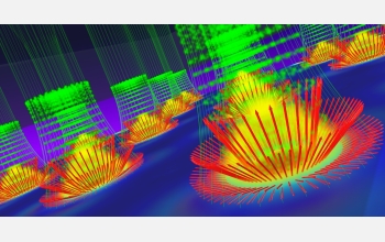
An overview of the Janko group's proposal for controlling a "spintronic" device.
This material is available primarily for archival purposes. Telephone numbers or other contact information may be out of date; please see current contact information at media contacts.

This animation gives an overview of the Janko group's proposal for controlling a "spintronic" device with superconductivity.
The idea is to create the device as a series of layers, each only a few dozen nanometers thick. At the bottom is a layer of diluted magnetic semiconductor (DMS) material--for example, gallium arsenide doped with manganese atoms. Each manganese atom contributes an extra electron to the material, and thus an extra electron spin. Above that is a layer of insulator (grey) and then a layer of superconducting material (SC).
Zooming in shows the magnetic field (green), which can thread through the superconducting layer only pinching itself down into an array of nanoscale flux tubes (green columns). The field in each flux tube is very intense, and extends right through the DMS layer. As it does, it forces a patch of electron spins to fall into line (red arrows). It also causes a certain amount of electric charge to accumulate (yellow).
Credit: Dr. Ovidiu Toader, University of Toronto

This video requires the free RealPlayer plug-in

