
Silicon Wafer Engineering & Defect Science Center (SiWEDS)
North Carolina State University (lead) and University of California at Berkeley
A National Science Foundation Industry/University Cooperative Research Center since 1997
A global partnership for research, development, and education
Center Mission and Rationale
The mission of the Center is to create a multi-university, multi-company culture that will address the critical non-competitive science and technology issues the international silicon materials industry requires to meet the future needs of advanced integrated circuit manufacturing. The education of graduate and postgraduate students in silicon materials engineering and defect science will be a critical component of the Center's activities. The Center's goals are to:
- Provide a mechanism for examining knowledge-based research issues of the wafer manufacturing community, which includes associated processing and measurement equipment suppliers, IC manufacturing companies, and raw materials suppliers
- Educate graduate and postgraduate students to become effective members of the wafer manufacturing research community with a minimal learning curve
- Provide a research and administrative infrastructure to enable the funding of large-scale, knowledge-based wafer engineering and defect science research.
|
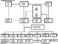
Center Organization
The Center membership includes those organizations and individuals who are committed to the Center vision and who participate actively in its implementation. At the time of publication, the Center has the following participants from the academic community:
- Arizona State University: Prof. D. Schroder
- University of Arizona, Prof. H. Parks
- UC Berkeley, Prof. E. Weber
- MIT, Prof. L. Kimerling
- University of Washington, Prof. S. Dunham
- Stanford University, Prof. P. Pianetta
- North Carolina State University, Prof. G. Rozgonyi
Our industrial membership includes a broad spectrum of major corporations ranging from silicon wafer vendors to integrated circuit manufacturers.
Prof. George Rozgonyi, of the Materials Science & Engineering Department of North Carolina State University, directs the Center and reports to the Dean of Engineering on all matters regarding Center administration. The Center Director receives advice on matters related to Center management and technical issues from an Industrial Advisory Board (IAB) composed of one representative from each of the Center industrial members. The IAB meets twice per year. Decisions made by the Center Director following consultation with and approval by the IAB membership are final.
Research Program
The technical work performed is divided into four task areas: Bulk Defects and Impurities; Surface Defects and Impurities; Developing Metrology Standards; and Formulating Models and Simulators for the various physical phenomena. Work on specific projects within a task area is normally performed by a combination of the various university groups, including graduate and postgraduate students, in collaboration with personnel from the Center member companies. The educational and technical mission of the Center is best served by strong interactions between the students and industrial mentors. New projects are established by the periodic submission of specific project white papers (proposals) to the IAB, which selects projects by assigning evaluation merit points. A key aspect of the approval process is the identification of potential research partnerships between the university and industrial members.
Special Center Activities
Education Programs
The main education program of the Center focuses on graduate and postgraduate students in areas related to the Center's technical activities in the overall wafer engineering and defect science area. The goal is to create an expanded population of scientists and engineers with the necessary skills and knowledge to become productive in the SiWEDS community with a minimum of on-site company training. This should help ensure a supply of future employees to the silicon materials industry. In addition to the normal educational programs associated with students, the Center provides opportunities for scientists and engineers of the member companies to enhance their knowledge in SiWEDS by serving as project mentors and visiting scientists at the university sites.
Technology Transfer
Center-developed knowledge and technology are transferred to members through five mechanisms: 1) the semi-annual two-day Center review meetings; 2) direct interactions with company scientists and engineers through research collaborations; 3) visits of faculty and Center students to member company facilities for one-on-one interactions; 4) the Center annual technical report; and 5) access to software and database developed at the university sites.
Stewardship and Outreach
More broadly, the Center provides an opportunity for the key scientific and technical issues of the silicon materials community to achieve a high level of visibility in the international semiconductor communities. The I/UCRC grant from the National Science Foundation (NSF) provides opportunities for additional research support from the NSF and other government funding agencies. In addition, a process has been developed, in consultation with the IAB, to include new supporting members from the industrial community and, as required, additional members from academia in order to expand the SiWEDS technical base of expertise.
Center Headquarters
Silicon Wafer Engineering & Defect Science Center (SiWEDS)
North Carolina State University
2149 Burlington Labs
Box 7916
Raleigh, NC 27695-7916
Tel: (919) 515-2933 * Fax (919) 513-1699
Homepage: www.mse.ncsu.edu/siweds/
Center Director: Prof. George A. Rozgonyi rozgonyi@ncsu.edu
Associate Director: Rene Gielen (919) 513-3927 * rene_gielen@ncsu.edu
Center Evaluator: Dr Denis Gray (919) 515-1721 * denis_gray@ncsu.edu
NSF 01-168mm