NSF/SRC Engineering Research Center for Environmentally Benign Semiconductor Manufacturing
University of Arizona (lead institution)
![]()
Leading a unique interdisciplinary collaboration to develop environmentally-friendly manufacturing processes and tools for the semiconductor industry
| A National Science Foundation Engineering Research Center since 1996 |
![]()
|
Partner Institutions:
|
In 1996, the University of Arizona (lead institution), Massachusetts Institute of Technology, Stanford University, and the University of California at Berkeley jointly established the NSF/SRC Engineering Research Center (ERC) for Environmentally Benign Semiconductor Manufacturing. In 1998, Cornell University, Arizona State University, and MIT's Lincoln Laboratory joined the Center to add additional capabilities for a new research thrust.
The purpose of the Center is to develop the science, technology, and educational methods necessary to lead the semiconductor industry to a new era of environmentally benign manufacturing. The goals and objectives of the Center are to:
- Develop a methodology for incorporating Environment, Safety & Health (ESH) factors in the design of new processes, tools, and protocols for semiconductor manufacturing
- Demonstrate this methodology by applying it to manufacturing processes that are of significant ESH concern
- Integrate the Center activities with academic programs to provide unique learning opportunities for undergraduate and graduate students
- Sponsor continuing education and industrial short courses, and outreach to high school teachers to improve science and math instruction and make teachers aware of industry employment opportunities
- Provide a technical forum for experts from industry, research institutions, and government agencies to exchange ideas and information on ESH concerns in semiconductor manufacturing.
Research
The semiconductor industry is a very fast-moving industry, creating many opportunities for innovation and change. The fast pace also presents a major challenge in planning and conducting long-term research to strike the right balance between long-term development, short-term relevance, and application to current problems. The Center's research strategy will be to maintain this balance and promote a mix of projects and activities ranging from high-risk, high-payoff research to smaller projects with more immediate applications.
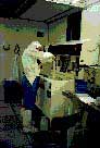 |
| Lab 1: Graduate student rinsing wafers in cleanroom laboratory. |
In today's semiconductor industry, environmental factors are not usually included in the design and development of new tools and processes. Integrating environmental technology into the design of processes and tools is the common theme of the Center's research.
The Center's interdisciplinary research efforts involve six universities, over 20 professors, more than 40 undergraduates, and 50 graduate students. The Center's research efforts are organized into four Thrusts, built around semiconductor manufacturing processes: A (Back End of Line Processes), B (Front End of Line Processes), C (Factory Water and Energy Use), and D (Patterning or Photolithography).
Thrust A (Massachusetts Institute of Technology, Stanford University, University of California at Berkeley, and University of Arizona) is pursuing the following research areas:
- Per-fluoro compound (PFC) alternatives for wafer patterning and chamber cleaning
- Solventless chemistries for deposition of low-k dielectric films
- Plasma abatement of HFC (hydro-fluoro compound) and PFC emissions
- CMP (chemical-mechanical polishing) wastewater minimization, recycling, and treatment.
Thrust B (Stanford University, University of Arizona, and Massachusetts Institute of Technology) is addressing the following:
- Development of environmentally benign wet (cleaning) processes
- Improvement of gate oxide integrity and function by reduction of surface roughness and contamination
- Removal of photoresist residues using environmentally friendly oxidants
- Gas-phase cleaning processes
- Extension of cleaning bath life through better process control, purification, and recycling.
Thrust C (University of Arizona and Stanford University) is working on:
- Development of new processes for ultra-pure water (UPW) generation and reuse
- Reducing process water usage and enhancing wafer rinsing performance
- Development of new processes and contaminant sensors for rinse water reuse and recycling.
Thrust D (Massachusetts Institute of Technology, Arizona State University, and Cornell University) focuses on:
- Development of solventless lithography for patterning integrated circuits (ICs)
- Identification of new, environmentally-friendly processes for creation of barrier and adhesion layers for low-k dielectric polymer thin films.
Education
The Center's education and outreach program encompasses university graduate and undergraduate students, high school teachers, and technical personnel in the semiconductor industry. The goal of the Center is to create a multi-disciplinary culture to attract and educate a new breed of engineering leaders for the semiconductor industry who will help it meet long-term environmental goals.
One of the objectives of the Center is to develop innovative educational programs at the university level to teach environmental factors as part of chemical and materials science and engineering courses. To do that, the Center has developed a new undergraduate lecture course, Microelectronics Manufacturing in the Environment.
To allow professors, students, and industrial partners at various locations to communicate effectively and benefit from an exchange of ideas, the Center holds a weekly teleseminar.
The Center offers a Research Experiences for Undergraduate (REU) Program that provides research internships for 10 students during the summer at participating universities. This program encourages students to enter graduate school and/or the semiconductor and environmental industries. The Center's outreach activities also focus on pre-engineering students and their teachers, offering activities designed to stimulate an interest in science and engineering. The Center has held a series of summer conferences and workshops for high school teachers at both Stanford University and the University of Arizona.
Since 1999, the Center has offered four industrial short courses on the Fundamentals of Chemical Mechanical Polishing (CMP), using both professors and industrial affiliates to teach the course.
Industrial Collaboration/Technology Transfer
The Center's strategy is to develop active partnerships with IC (Integrated Circuit) manufacturers, SEMATECH, and equipment suppliers to ensure that the technology developed at the Center is transferred in a timely and effective manner.
One successful example is the transfer of reactive filter technology developed at the University of Arizona to the Pall Corporation, leading to commercialization of the Pall part per trillion (ppt) filter-purifier only three years after the research began.
The Center facilitates technology transfer through industrial internships for students, industrial sabbaticals for the university faculty, educational sabbaticals for industrial personnel, and joint research and teaching projects.
The Center currently has 30 industrial partners on its Industrial Advisory Board (IAB). The advisors participate actively in our weekly teleconferences and our annual IAB retreats. The advisors also mentor our graduate students.
Facilities
Each of the six universities involved in the Center provides laboratories, equipment, and other facilities that are used for Center activities.
University of Arizona
Center offices are located at the University of Arizona. The space includes faculty offices, staff offices, a library/reading room, and a conference room. In addition, U of A's laboratory facilities include: a semiconductor fabrication facility (including a class 1000 cleanroom); a complete Ultrapure Water Pilot Research Laboratory; a nanofabrication facility; and an integrated optics characterization laboratory.
Massachusetts Institute of Technology
MIT's Microsystems Technology Laboratories is home to two principal plasma research tools: an Applied Materials Precision 5000 etch tool and a Novellus Concept One PECVD tool. Also at MIT is the Center for Materials Science and Engineering (CMSE), a shared analytical facility possessing an extensive inventory of materials analysis equipment.
MIT also possesses a parallel plate rf plasma reactor for pulsed PECVD (plasma enhanced chemical vapor deposition), ECR Reactor for pulsed PECVD, two Solid-State NMR Spectrometers for thin film characterization, and MIT Lincoln Labs (VUV Spectrophotometer for measuring film absorbances).
Stanford University
Stanford's Center for Integrated Systems has a variety of plasma processing equipment, including: a 3-chamber Applied Materials 5000 etcher; a Lam TCP polysilicon etcher; an STS ICP etcher; a PlasmaQuest ECR etcher; and an STS plasma deposition system. In Stanford's Paul Allen Extension to the Center for Integrated Systems, about 1800 sq. ft. of H7 class laboratory has been allocated to the Center for ultra-clean processing and characterization.
University of California at Berkeley
UC-Berkeley has a variety of experimental equipment including: two experimental ICP (inductive coupled plasma) systems; an experimental vacuum-beam system; and a high-density plasma-oxide etch system (TCP transformer coupled plasma).
Cornell University
Cornell University has the following research facilities: the Cornell Nanofabrication Facility (clean room facilities for lithographic processing); the Cornell Center for Materials Research (Ion Beam Facility for Rutherford Backscattering Spectrometry studies); and the Advanced Electronic Packaging Facility (houses supercritical fluid chamber for CO2 development).
Arizona State University
ASU has the following equipment used in the Center's research: a vapor deposition polymerization system; a remote microwave plasma system; an Atomic Force Microscope (AFM); a Fourier Transform infrared spectrometer (FTIR); and a Field emission gun scanning electron microscope (FEG-SEM).
Center Configuration, Leadership, and Team Structure
The Center management consists of the Center Director (Farhang Shadman, University of Arizona), the Associate Director (Rafael Reif, MIT), and the Executive Committee. The Executive Committee consists of Farhang Shadman from U of A, Rafael Reif from MIT, and Krishna Saraswat from Stanford, along with the Thrust Leaders, the Education Coordinator, and the Industrial Liaison Officer.
The Executive Committee oversees all aspects of the Center operation in research, teaching, and education. It plans the Center's growth, monitors the progress of all Thrust Areas and their collaboration and interaction, plans the Center's industrial relationships and outreach, and plans the priorities.
Thrust Area leaders are responsible for all aspects of their individual research Thrust Area activities, including budgeting and monitoring progress according to goals and milestones, preparing reports, coordinating projects, and recruiting new investigators and projects.
Two advisory boards, the Policy Board and the Industrial Advisory Board, guide the operation of the Center. The Policy Board is comprised of Deans of Engineering or their representatives from participating universities, senior managers from industry, other distinguished technical experts, and the Center Director. The Policy Board ensures that the overall activities of the Center are carried out as per approved NSF/SRC policy guidelines. The Industrial Advisory Board is a team of experts from industry, academia, and National Laboratories who advise the Executive Committee on Center programs, strategic plans, and annual operational and technical plans, as well as on linkage to industry and technology transfer.
![]()
Center Headquarters
NSF/SRC Engineering Research Center for Environmentally Benign Semiconductor
Manufacturing
Chemical and Environmental Engineering
The University of Arizona
Tucson, AZ 85721
Tel (520) 621-6051 · Fax (520) 626-5397
Homepage: http://www.erc.arizona.edu
Center Director: Prof. Farhang Shadman
shadman@erc.arizona.edu
Associate Director: Prof. Rafael Reif
reif@mtl.mit.edu
NSF 00-137h