
All Images
News Release 12-164
Engineering Research Centers Awarded $55.5M to Innovate in Nanoscale Science and Engineering
Three new centers to address significant national needs: health and environmental monitoring, mobile computing and energy technologies, and electromagnetic components
This material is available primarily for archival purposes. Telephone numbers or other contact information may be out of date; please see current contact information at media contacts.
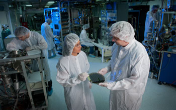
ASSIST Center Director Dr. Veena Misra (center left) and Deputy Director Dr. John Muth (center right) are pictured in the Nanostructures Laboratory at North Carolina State University. The ASSIST Center, an NSF Nanosystems Engineering Research Center (NERC) begun in 2012, brings together researchers at NCSU and partner institutions to create self-powered devices that help people monitor their health and understand how it is affected by their environment.
Credit: Marc Hall, North Carolina State University
Download the high-resolution JPG version of the image. (5.6 MB)
Use your mouse to right-click (Mac users may need to Ctrl-click) the link above and choose the option that will save the file or target to your computer.
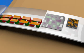
Researchers in the ASSIST Center, an NSF Nanosystems Engineering Research Center, will use nanomaterials and nanodevices to develop self-powered health monitoring systems. Some of these devices could be worn on the wrist, like a watch.
Credit: Illustrated by Narayanan Ramanan, North Carolina State University
Download the high-resolution JPG version of the image. (964 KB)
Use your mouse to right-click (Mac users may need to Ctrl-click) the link above and choose the option that will save the file or target to your computer.

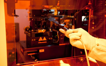
Wafer-scale nanopatterning is used in the fabrication of photonic crystal structures for light emitting diodes or LEDs. Creating nanomanufacturing process systems that are high-throughput, reliable and versatile is the focus of the NSF Nanosystems Engineering Research Center led by the University of Texas, called the Center for Nanomanufacturing Systems for Mobile Computing and Mobile Energy Technologies or NASCENT.
Credit: Cockrell School of Engineering, University of Texas at Austin
Download the high-resolution JPG version of the image. (123 KB)
Use your mouse to right-click (Mac users may need to Ctrl-click) the link above and choose the option that will save the file or target to your computer.
A researcher loads a template that serves as a master for nano-sculpting on plastic films in a roll-to-roll tool. The template is a glass wafer that is etched with the desired nanoscale features. With advances in nanoscale manufacturing and systems, NASCENT researchers aim to make the performance promised by nanomaterials and nanotechnologies more widely available and economically competitive.
Credit: Cockrell School of Engineering, University of Texas at Austin
Download the high-resolution JPG version of the image. (3.5 MB)
Use your mouse to right-click (Mac users may need to Ctrl-click) the link above and choose the option that will save the file or target to your computer.
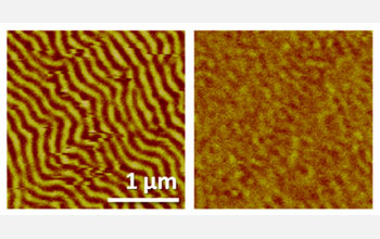
TANMS researchers have used an electric field to turn a magnetic field on (left) and off (right). They measured this effect in a ferromagnetic thin film on top of a piezoelectric substrate, using a magnetic force microscope. At left, the dark lines represent magnetic north poles emanating from the ferromagnetic thin film, and the light lines represent magnetic south poles. At right, an electric field is applied to the piezoelectric substrate, and the lines vanish, meaning that the magnetic field is no longer present. The researchers will expand on this ability to control magnetic fields in nanostructured ferromagnetic elements in the work of the TANMS Nanosystems Engineering Research Center. TANMS seeks to integrate newly discovered large-effect multiferroic materials into electromagnetic devices, thereby enabling chip-scale generation of magnetic fields through the simple application of a voltage. Their research could lead to transformations in memory systems, antenna systems, and nanomotor systems.
Credit: Ray C. J. Hsu, Mechanical and Aerospace Engineering, University of California Los Angeles
Download the high-resolution JPG version of the image. (188 KB)
Use your mouse to right-click (Mac users may need to Ctrl-click) the link above and choose the option that will save the file or target to your computer.
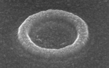
This Scanning Electron Micrograph shows a 500nm nickel ring on a piezoelectric substrate. Such ferromagnetic rings may be used in the fabrication of nanoscale motors at the NSF Nanosystems Engineering Research Center for Translational Applications of Nanoscale Multiferroic Systems.
Credit: Joshua Leon Hockel, Mechanical and Aerospace Engineering Department, University of California Los Angeles
Download the high-resolution JPG version of the image. (532 KB)
Use your mouse to right-click (Mac users may need to Ctrl-click) the link above and choose the option that will save the file or target to your computer.