
Multimedia Gallery
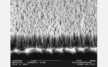
ZnO nanotips grown on C-plane sapphire substrates
A scanning electron microscope (SEM) image showing ZnO nanotips grown on C-plane sapphire substrates.
This work was supported by National Science Foundation grant CCR 01-03096, "Feasibility studies on ZnO nanostructures and their device applications," an exploratory research in the Nanoscale Science and Engineering Initiative. Project goals were to (a) grow ZnO-based nanoscale structures, including nanotips and nanotip arrays, nanowires and quantum dots; and (b) investigate the broad applications of these ZnO nanostructures in UV optoelectronics, biosensors and advanced communications. The ZnO materials are grown using metalorganic chemical vapor deposition.
Credit: Dr. Yicheng Lu, Dr. Sriram Muthukumar and Dr. Nuri Emanetoglu, Department of Electrical and Computer Engineering, Rutgers University
Images and other media in the National Science Foundation Multimedia Gallery are available for use in print and electronic material by NSF employees, members of the media, university staff, teachers and the general public. All media in the gallery are intended for personal, educational and nonprofit/non-commercial use only.
Images credited to the National Science Foundation, a federal agency, are in the public domain. The images were created by employees of the United States Government as part of their official duties or prepared by contractors as "works for hire" for NSF. You may freely use NSF-credited images and, at your discretion, credit NSF with a "Courtesy: National Science Foundation" notation.
Additional information about general usage can be found in Conditions.
Also Available:
Download the high-resolution JPG version of the image. (186 KB)
Use your mouse to right-click (Mac users may need to Ctrl-click) the link above and choose the option that will save the file or target to your computer.