
Multimedia Gallery
 All images in this series
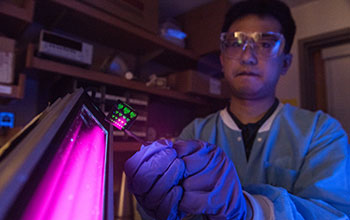
Ultraviolet light used by technique to impart a pattern
Researchers have developed a new technique, called DOLFIN, that makes it easier to build nanomaterials into transistors, solar cells and other devices Exposure to ultraviolet light can be used as part of the DOLFIN technique to impart a pattern.
More about this image
Scientists at the University of Chicago and Argonne National Laboratory have discovered a new way to precisely pattern nanomaterials that could open a new path to the next generation of everyday electronic devices. The new technique is expected to make such materials easily available for eventual use in everything from LED displays to cellular phones to photodetectors and solar cells.
While nanomaterials are promising for future devices, ways to build them into complex structures have been limited and small scale.
The foundation of modern computing are tiny switches, called transistors, created by a technique called photolithography. Photolithography carves a stencil out of a layer of organic polymer by laying down a patterned "mask" and illuminating it with ultraviolet light. After the new material is deposited on top, the polymer stencil is lifted off to reveal the pattern. Several rounds of such patterning build a miniature transistor onto the material. The new technique, called DOLFIN, makes different nanomaterials directly into "ink" in a process that bypasses the need to lay down a polymer stencil.
"This is a step needed to move quantum dots and many other nanomaterials from proof-of-concept experiments to real technology we can use," said Dmitri Talapin, professor of chemistry at UChicago and a scientist with the Center for Nanoscale Materials at Argonne. "It really expands our horizons."
The work was supported by the U.S. National Science Foundation (grants CHE 1611331 and the NSF Materials Research Science and Engineering Center Program under award DMR 1420709).
To learn more about this research, see the NSF News From the Field story New method promises easier nanoscale manufacturing. (Date image taken: July 2017; date originally posted to NSF Multimedia Gallery: Jan. 25, 2018)
Credit: Photo courtesy of The University of Chicago/Jean Lachat
See other images like this on your iPhone or iPad download NSF Science Zone on the Apple App Store.
Images and other media in the National Science Foundation Multimedia Gallery are available for use in print and electronic material by NSF employees, members of the media, university staff, teachers and the general public. All media in the gallery are intended for personal, educational and nonprofit/non-commercial use only.
Images credited to the National Science Foundation, a federal agency, are in the public domain. The images were created by employees of the United States Government as part of their official duties or prepared by contractors as "works for hire" for NSF. You may freely use NSF-credited images and, at your discretion, credit NSF with a "Courtesy: National Science Foundation" notation.
Additional information about general usage can be found in Conditions.
Also Available:
Download the high-resolution JPG version of the image. (10.9 MB)
Use your mouse to right-click (Mac users may need to Ctrl-click) the link above and choose the option that will save the file or target to your computer.