
All Images
Research News
Plasma Waves Studied for New Electronics

In the lab, William Stillman evaluates the effects of focused terahertz (THz) radiation on very-large-scale integration (VLSI) ring oscillator circuits. (At the right, in the foreground, is the 0.2 THz Gunn oscillator source. Instruments in the center are an oscilloscope, spectrum analyzer and lock-in amplifier.)
Credit: William Stillman, Rensselaer Polytechnic Institute
Download the high-resolution JPG version of the image. (265 KB)
Use your mouse to right-click (Mac users may need to Ctrl-click) the link above and choose the option that will save the file or target to your computer.
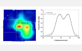
A 0.2 terahertz (THz) response map (left) and detector response simulation (right) for a 120 nanometer field-effect transistor (NFET). The detector dimensions used to achieve the best fit to measured data are in the range of the radiation wavelength of 1.5 millimeters.
Credit: William Stillman, Rensselaer Polytechnic Institute
Download the high-resolution JPG version of the image. (205 KB)
Use your mouse to right-click (Mac users may need to Ctrl-click) the link above and choose the option that will save the file or target to your computer.
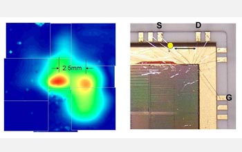
A 0.2 terahertz (THz) response map (left) and test device photograph showing approximate peak locations (right). The relatively long wavelength of the 0.2 THz radiation tends to couple to the circuit bonding wires, which act as antennas.
Credit: William Stillman, Rensselaer Polytechnic Institute
Download the high-resolution JPG version of the image. (168 KB)
Use your mouse to right-click (Mac users may need to Ctrl-click) the link above and choose the option that will save the file or target to your computer.