
All Images
Research News
Miracle Material
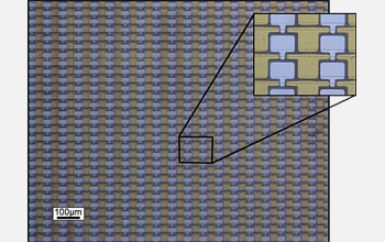
Optical micrograph of an array of graphene transistors prepared on silicon carbide (SiC). There are 40,000 devices per square centimeter.
Credit: M. Sprinkle, M. Ruan,Y. Hu, J. Hankinson,M. Rubio-Roy, B. Zhang, X. Wu, C. Berger & W. A. de Heer. (2010). Scalable templated growth of graphene nanoribbons on SiC. Nature Nanotechnology (5), 727-731.
Download the high-resolution JPG version of the image. (181 KB)
Use your mouse to right-click (Mac users may need to Ctrl-click) the link above and choose the option that will save the file or target to your computer.

Georgia Tech graduate students Yike Hu and John Hankinson observe a high-temperature furnace used to produce graphene on a silicon wafer.
Credit: Gary Meek, Georgia Institute of Technology
Download the high-resolution JPG version of the image. (1.2 MB)
Use your mouse to right-click (Mac users may need to Ctrl-click) the link above and choose the option that will save the file or target to your computer.
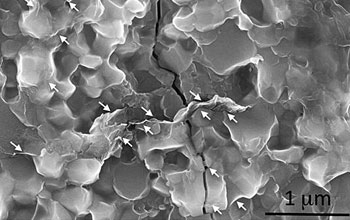
Wrapping of graphene platelets around silicon nitride grain boundaries. The graphene platelets are able to deflect propagating cracks thereby toughening the ceramic by over 200 percent.
Credit: Nikhil Koratkar, Rensselaer Polytechnic Institute and Erica Corral, University of Arizona
Download the high-resolution JPG version of the image. (105 KB)
Use your mouse to right-click (Mac users may need to Ctrl-click) the link above and choose the option that will save the file or target to your computer.